Knight Rider Circuit
This circuit mimics the lights in knight rider's car. They flash one at a time chasing each other.
Overview
In the
Knight Rider circuit, the 555 is wired as an oscillator. It can
be adjusted to give the desired speed for the display. The output of
the 555 is directly connected to the input of a Johnson Counter (CD
4017). The input of the counter is called the CLOCK line.
The 10 outputs Q0 to Q9 become active, one at a time, on the rising edge of the waveform from the 555. Each output can deliver about 20mA but a LED should not be connected to the output without a current-limiting resistor (330R in the circuit above).
The first 6 outputs of the chip are connected directly to the 6 LEDs and these "move" across the display. The next 4 outputs move the effect in the opposite direction and the cycle repeats. The animation above shows how the effect appears on the display.
Using six 3mm LEDs, the display can be placed in the front of a model car to give a very realistic effect. The same outputs can be taken to driver transistors to produce a larger version of the display.

The input of the 4017 counter is called the CLOCK line. The 10 outputs Q0 to Q9 become active, one at a time, on the rising edge of the waveform from the 555.
IC 555 data sheet
555 Timer Internal Circuit Block Diagram

555 Timer Internal Circuit Block Diagram


The output of a 555 timer is either high (close to +VCC) or low (close to GND).
Inside the 555 timer is a voltage divider the divides +VCC into thirds. A voltage comparator compares the trigger input (pin 2) with 1/3 VCC, and another comparator compares the threshold (pin 6) with 2/3 VCC. The point at 2/3 VCC on the voltage divider is connected to the control voltage (pin 5). This pin can be used to modify the values of 1/3 VCC and 2/3 VCC without having to change VCC. However, if this input is not going to be used, it should be grounded through a bypass capacitor (0.01uF) to protect it from noise.
The 555 timer also has a flip-flop, which is controlled by the two comparators and the reset input.
The trigger and reset inputs are level-sensitive active low inputs. To activate the trigger, the voltage on the trigger pin must be pulled down to under 1/3 VCC. The trigger experiences a delay when changing states so it should be returned to high at least 10μs before the end of the timing cycle or else the cycle will be immediately re-triggered.
To reset the timer, the voltage on the reset pin must be pulled under 0.4V. The reset input will override other inputs and set the output (pin 3) to low. If the reset input is not going to be used, it should be wired to VCC to prevent false signals.
In its initial state (assuming threshold is low and trigger is high), the 555 timer's internal flip-flop connects the discharge (pin 7) to the ground and sets the output to low. Each time the trigger voltage is pulled down under 1/3 VCC, the flip-flop will break the discharge pin's connection to ground, and set the output to high. It will hold this state until something (usually a capacitor) forces the threshold pin's voltage equal to 2/3 VCC, which will reset the flip-flop.
555 Pins

Monostable and Astable mode
The 555 family of timer chips can be used in either monostable mode or astable mode. In the monostable or "one shot" mode, each time the 555 timer is triggered, the output will go high for a specified amount of time, then return to low
and await another trigger signal. In the astable mode, the timer
triggers itself periodically and becomes an oscillator, sending out a
train of pulses.
Monostable Mode
Connections for the 555 timer in monostable mode:

- In this circuit's initial condition, the capacitor C is held discharged through the discharge pin, which is grounded through the flip-flop in the timer. The threshold voltage is equal to the voltage across the capacitor.
- When the trigger pin receives a negative trigger pulse less than 1/3 VCC, the flip-flop sets the output to high and disconnects the discharge pin from the ground. This allows the capacitor to charge until the voltage across it reaches 2/3 VCC, which takes about t=1.1RAC seconds.
- When the threshold voltage reaches 2/3 VCC, the flip-flop resets, connecting discharge to the ground and setting output to low. It is now back in the initial state, and awaits another trigger pulse.
Timing diagram for the 555 in monostable mode:

Astable mode
astable mode, the circuit will keep re-triggering
itself, resulting in a pulse train. The circuit for the 555 in astable
mode looks like this:

the capacitor charges and discharges between 1/3 VCC and 2/3 VCC. The 555's output will the high while charging, and low while discharging. The capacitor charges and discharge at different rate—it has to charge through RA and RB, but it only discharges through RB. Thus, we can adjust the length of the output's highs and lows by adjusting these resistors.
The length of a output high is equal to:

The timing diagram for the 555 in astable mode:

555 applications
single 555 for flashing the display cursor.
4017 IC Datasheet
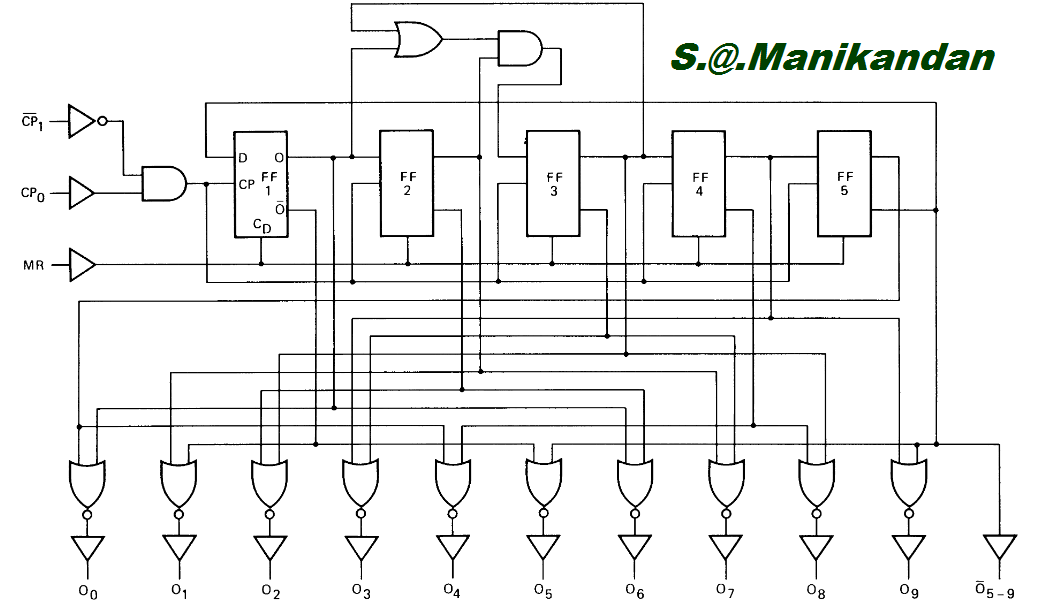
4017 IC is a CMOS counter/divider integrated circuit, actually a decada
counter with 10 decode ouputs. It is 5 stage Johnson counters having 10
decoded outputs. Inputs include a clock, a reset, and a clock inhibit
signal.
The CD4017BC is a 5-stage divide-by-10 Johnson counter with 10 decoded outputs and a carry out bit.
The CD4022BC is a 4-stage divide-by-8 Johnson counter with 8 decoded outputs and a carry-out bit.
These counters are cleared to their zero count by a logical “1” on their reset line. These counters are advanced on the positive edge of the clock signal when the clock enable signal is in the logical “0” state.
The configuration of the CD4017BC and CD4022BC permits medium speed operation and assures a hazard free counting sequence. The 10/8 decoded outputs are normally in the logical “0” state and go to the logical “1” state only at their respective time slot. Each decoded output remains high for 1 full clock cycle.The carry-out signal completes a full cycle for every 10/8 clock input cycles and is used as a ripple carry signal to any succeeding stages
Wide supply voltage range: 3.0V to 15V
High noise immunity: 0.45 VDD (typ.)
Low power Fan out of 2 driving 74L TTL compatibility: or 1 driving 74LS
Medium speed operation: 5.0 MHz (typ.) with 10V VDD
Low power: 10 mW (typ.)
Fully static operation
Applications
• Automotive
• Instrumentation
• Medical electronics
• Alarm systems
• Industrial electronics
• Remote metering
• Instrumentation
• Medical electronics
• Alarm systems
• Industrial electronics
• Remote metering
Pin Diagrams

Functional diagram

Logic diagram
Timing diagram

No comments :
Post a Comment