Tuesday, 10 September 2019

12 Volt DC to 220 Volt AC 100 Watt Converter $ Home Made


                          12 Volt DC to 220 Volt AC 100 Watt Converter & 12 volt to 24 volt converter
                        

                                                           Inside Box


                                                           Front View


                                                             Back View


                                                               Circuit Diagram


Highlights
  • Can Convert DC 12V into AC 220V Output.
  • Can be Directly Used for MP3 Player, Mobile Phone Charger , LED Light, Color TV, DTH Box & CFL from any 12V DC Power Source.  
  • 12V DC to 220V AC, 100Watt
Description
The DC Converter widely used for all kinds of electric equipment where power consumption and voltage requirements are equal to AC 220 V. Equipment’s such as Cell-Phone, Portable Computer, Electric Light, Digital Camera, TV, CD player, DVD, Electric Tool, CLF, Mobile Charger , LED Light and so on are powered by this unit. It converts DC 12V electricity source into AC 220V power.
Features:

·         It can convert DC 12V into AC 220V output 100 Watt.
·         Safely Shuts down in Over Temperature or Over Load Conditions

Please Note:

´         This Unit Not Work with any Type of Fan, Ceiling Fan, Motor or Pump.
´         Don’t Operate Any Transformer Based Device with This Unit.

 Please Note:

      this is an inverter making circuit diagram, here we are using only two MOSFET because it’s only 100 watts inverter. we use the ic ka3525a ( sg3525 equivalent Ic) for the oscillation. in this circuit only can load 100 watts. if we want to increase the watts then we have to use add more transistor and need a big transformer. the circuit diagram can be the same. after the ziner diode, we have to add extra MOSFET. 


Sunday, 5 November 2017

LA76931 Data Voltage & TN government free tv circuit

Data IC

LA76931  Data Voltage

PIN 1. SIF OUTPUT 2.4V
PIN 2. IF AGC FILTER 0V
PIN 3. SIF INPUT 3.1V
PIN 4. FM FILTER 2.3V
PIN 5. FM OUTPUT 2.6V
PIN 6. OUTPUT AUDIO TO SOUND AMPLIFIER AUDIO 2.3V
PIN 7. SND APC FILTER 2.3V
PIN 8. IF VCC 5V
PIN 9. EXT AUDIO IN 2.4V
PIN 10. ABL IN 3.7V
PIN 11. RGB VCC 8.4V
PIN 12. R OUTPUT 1.6V
PIN 13. G OUTPUT 1.8V
PIN 14. B OUTPUT 3.4V
PIN 15. N.C
PIN 16. V.RAMP 2.1V
PIN 17. V.OUTPUT 2.6V
PIN 18. VCO I REF 1.5V
PIN 19. HORIZONTAL VCC 5V
PIN 20. AFC FILTER 2.6V
PIN 21. H.OUTPUT 0.7V
PIN 22. GND
PIN 23. MUTE 1.7V
PIN 24. N.C
PIN 25. N.C
PIN 26. I.R IN/SENSOR I.R IN 3V
PIN 27. N.C
PIN 28. N.C
PIN 29. 2.9V
PIN 30. POWER ON/OFF ON 5V OFF 0V
PIN 31. SDA 4.8V
PIN 32. SCL 4.8V
PIN 33. XTALL IN 2V/32.768KHZ
PIN 34. XTALL OUT 3V/32.768KHZ
PIN 35. CPU VCC 5V
PIN 36. KEY IN/PANEL SWITCH 4.8V
PIN 37. VL 0V
PIN 38. VH 0V
PIN 39. UHF 5V
PIN 40. RESET 4.8V
PIN 41. PLL 3V
PIN 42. GND
PIN 43. CDD VCC 4.6V
PIN 44. FBP IN 0.5V
PIN 45. N.C
PIN 46. N.C
PIN 47. DDS FILTER 1.1V
PIN 48. N.C
PIN 49. 2.1V
PIN 50. XTALL 4.43 4V
PIN 51. CR.IN 2.3V
PIN 52. VIDEO OUTPUT 2.2V
PIN 53. APC FILTER 3.4V
PIN 54. EXT VIDEO IN 2.5V
PIN 55. VCC 5V
PIN 56. V. IN TV 3.5V
PIN 57. BLACK STRETCH FILTER 2.3V
PIN 58. PIF APC FILTER 2.8V
PIN 59. AFT OUTPUT 0.2V
PIN 60. V.OUTPUT TV 3.5V
PIN 61. RF AGC TUNER 4V
PIN 62. GND
PIN 63. VIF IN2 2.9V
PIN 64. VIF IN1 2.9V

S.M.P.S Transistor

C4458 transistor
C3807 transistor

TV Dead-Repaired

Initial test: Television is totally dead.

I opened the TV and went straight to the safety components; I started with the main fuse, found to have had catastrophic failure that even the glass part of the fuse was broken.
Once I found the fuse has died catastrophically, next I moved to check the state of the switching transistor.


Upon testing it with my digital meter set to diode test, I got a beep either way, the resistance was near to zero.
Then I concluded this component has gone also-please note that if this transistor short expects the fuse or the surge limiter to open.


To confirm the switching transistor was actually shorted I cut its middle leg (collector) with a side cutter and tested across the C-E pins again, there was still a beep (short indication)


Next I moved to the secondary side, I tested across the secondary side diodes with the meter probe on one side and then reversed the probe.
I noticed when testing across the main B+ diode rectifier there was a beep either way, This is an indication that the actual diode is shorted or a component along that line.
To confirm, I cut one leg of this diode and tested across it again I got no beep. This confirmed to me that this diode is okay and therefore I should concentrate on the component after this diode.


 The main suspect now is after this diode is the H.O.T, testing across the C-E junction of this transistor; I got beep on either way of the meter probe.


Again I suspected it is the culprit, to confirm I cut the middle leg from the circuit and upon testing the again the C-E pins with one leg (collector) removed from the circuit, the transistor was found to be okay.
Then I suspected the flyback as you can see from the above diagram it is also on direct path with the suspect line (B+) and to be sure it was the one shorted, I decided to remove it completely from the board.
This I did and after testing across the C-E (on the circuit track with the middle leg of H.O.T transistor lifted up from the circuit board) sadly I was again wrong. The short was still present.
So what next? I pulled my ESR meter to assist me to locate the shorted component.
With one probe of the ESR meter on the collector(C) pin of the HOT transistor, I followed the circuit track from the pin E(emitter) and going forward I noticed the ESR value was decreasing steadily and the lowest reading was recorded at both legs of capacitor C416 which was number 470p/2kV


I pulled my digital meter to confirm and indeed this capacitor was dead short.
I soldered one of it leg out and testing again across the C-E junction of the HOT, this time I never got the beep and this confirmed to me that indeed this was the culprit.
I got another from the junk board and I replaced it, I also replaced the switching transistor and re-installed the FBT and now was the time to apply the power which of course was via the series bulb.
After applying the power I noticed the bulb was very bright and was not going dim and this concluded to me that there is still a shorted component.
I tested the voltage across the main capacitor and the reading was 64 vdc.
This could point to a problem with the diode rectifier and I tested with a meter in diode mode and for sure I found one of the four (4) diodes was shorted and replaced it.
I was now smiling because I figured that this is the end of this assignment but again I was wrong.
After replacing the diode I tested across the main capacitor and still the voltage was very low and the series bulb was still very bright which is still a sign of present of a shorted component on the supply.
So decided to do component by component testing for the entire primary side components.
From my experience I decided to start with all the diodes and all diodes were found to be healthy according to my digital meter.
Next I checked the transistors and I decided to start with the transistor C3807 which drive the switching transistor.
This transistor has its collector pin connected to the base of the switching transistor.
I tested between the C-E junction of this small transistor and I got a beep, I reversed the probe and still got a beep.
I guessed maybe it is because I am doing the testing in-circuit and hence decided to remove this transistor out of the circuit and upon testing it out of the circuit still there was a beep and therefore I concluded the transistor is shorted.
I took another and replaced it and again applied power via the series bulb and this time the bulb was dim.


This confirmed to me that there is no other shorted component on the supply.
Later I went to the owner of this board and after re-installing the board back to the tube the TVcame back to life.
Lessons learn: whenever you change the switching transistor kindly change the drive transistor also directly.
Usually when the switching transistor get shorted this small driver transistor connected to its base short also or get a lot of stress and therefore even if you find it okay it is a matter of time before it succumb.
Conclusion: After doing replacement of all the parts in this television I figured out what could have really happened to cause this kind of damage to these components and this is how I figured out to have happened (postmortem).
First I suspect the problem started with small capacitor (470p/2kV) on the B+ line which developed a short.
After shorting the B+ voltage which is highly regulated at 109 VDC dropped drastically.
At this time the feedback circuit unaware of what has happened communicated to the primary side that we need more voltage on the secondary side and this then made the switching transistor to switch very fast to correct the short fall in the B+ voltage…this transistor was then overdriven and eventually surrendered (shorted), this also affected the driver transistor and also got shorted.
All this time the main fuse was still hanging on and then next one of the diode rectifiers also got shorted.
After this the main fuse had no choice but to also give in and because of many shorted component on the supply it has to go catastrophically…and hence the power was cut from damaging more components…the all process could have taken less than four (4) seconds.


Wednesday, 12 March 2014

ALL Remote Tester Circuit

Description.

This is a simple remote controller tester circuit  based on infrared sensor IC TSOP 1738. TSOP 1836.etc When the IR waves fall on the sensor it output changes to low state.This makes the transistor Q1 ON and LED will blink according to the code contained in the signal. So for press of each button the LED blinks in different ways. This is a good indication of the working of remote.

                                                                            Remote Tester Circuit

Notes .

 This circuit can be used to test remotes operating in the 38Khz carrier frequency.Almost all remotes fall into this category so no problem.

 Examples

TV remote,USB & AC and others

Sensor Type

Following the specification of component
 Transistor BC557,BC556
TSOP 1736 Sensor Infra Red
R1 = 330 ohm ¼ watt Resistor
R2 = 10k ohm ¼ watt Resistor
R3 = 1k ohm ¼ watt Resistor
led

Transistor BC557 data sheet


FEATURES

Low current (max. 100mA)
Low voltage (max. 65V).

APPLICATIONS

General purpose switching and amplification.

DESCRIPTION

PNP transistor in a TO-92; SOT54 plastic package. 
BC557 Pin


Please try I am sure 100% will be successful.


Wednesday, 19 February 2014

Led Knight Rider Circuit

Knight Rider Circuit

This circuit mimics the lights in knight rider's car. They flash one at a time chasing each other.

Overview

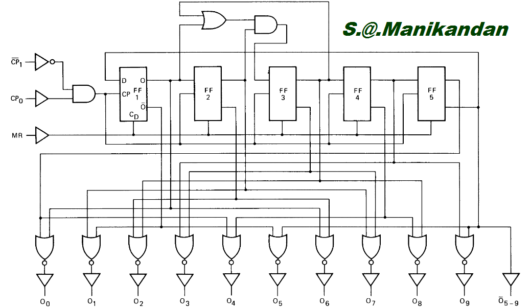
In the Knight Rider circuit, the 555 is wired as an oscillator. It can be adjusted to give the desired speed for the display. The output of the 555 is directly connected to the input of a Johnson Counter (CD 4017). The input of the counter is called the CLOCK line.
The 10 outputs Q0 to Q9 become active, one at a time, on the rising edge of the waveform from the 555. Each output can deliver about 20mA but a LED should not be connected to the output without a current-limiting resistor (330R in the circuit above).
The first 6 outputs of the chip are connected directly to the 6 LEDs and these "move" across the display. The next 4 outputs move the effect in the opposite direction and the cycle repeats. The animation above shows how the effect appears on the display.
Using six 3mm LEDs, the display can be placed in the front of a model car to give a very realistic effect. The same outputs can be taken to driver transistors to produce a larger version of the display.
In the Knight Rider circuit, the 555 is wired as an oscillator (Astable mode). The output of the 555 is directly connected to the input of a 4017 decade counter.

The input of the 4017 counter is called the CLOCK line. The 10 outputs Q0 to Q9 become active, one at a time, on the rising edge of the waveform from the 555.

IC 555 data sheet

555 Timer Internal Circuit Block Diagram


555 Timer Internal Circuit Block Diagram


See the Datasheet for the LM555 for more information and example applications/circuits.
The output of a 555 timer is either high (close to +VCC) or low (close to GND).
Inside the 555 timer is a voltage divider the divides +VCC into thirds. A voltage comparator compares the trigger input (pin 2) with 1/3 VCC, and another comparator compares the threshold (pin 6) with 2/3 VCC. The point at 2/3 VCC on the voltage divider is connected to the control voltage (pin 5). This pin can be used to modify the values of 1/3 VCC and 2/3 VCC without having to change VCC. However, if this input is not going to be used, it should be grounded through a bypass capacitor (0.01uF) to protect it from noise.
The 555 timer also has a flip-flop, which is controlled by the two comparators and the reset input.
The trigger and reset inputs are level-sensitive active low inputs. To activate the trigger, the voltage on the trigger pin must be pulled down to under 1/3 VCC. The trigger experiences a delay when changing states so it should be returned to high at least 10μs before the end of the timing cycle or else the cycle will be immediately re-triggered.
To reset the timer, the voltage on the reset pin must be pulled under 0.4V. The reset input will override other inputs and set the output (pin 3) to low. If the reset input is not going to be used, it should be wired to VCC to prevent false signals.
In its initial state (assuming threshold is low and trigger is high), the 555 timer's internal flip-flop connects the discharge (pin 7) to the ground and sets the output to low. Each time the trigger voltage is pulled down under 1/3 VCC, the flip-flop will break the discharge pin's connection to ground, and set the output to high. It will hold this state until something (usually a capacitor) forces the threshold pin's voltage equal to 2/3 VCC, which will reset the flip-flop.


555 Pins

Monostable and Astable mode

The 555 family of timer chips can be used in either monostable mode or astable mode. In the monostable or "one shot" mode, each time the 555 timer is triggered, the output will go high for a specified amount of time, then return to low and await another trigger signal. In the astable mode, the timer triggers itself periodically and becomes an oscillator, sending out a train of pulses.  

Monostable Mode

Connections for the 555 timer in monostable mode:  
The circuit operates as follows:
  1. In this circuit's initial condition, the capacitor C is held discharged through the discharge pin, which is grounded through the flip-flop in the timer. The threshold voltage is equal to the voltage across the capacitor.
  2. When the trigger pin receives a negative trigger pulse less than 1/3 VCC, the flip-flop sets the output to high and disconnects the discharge pin from the ground. This allows the capacitor to charge until the voltage across it reaches 2/3 VCC, which takes about t=1.1RAC seconds.
  3. When the threshold voltage reaches 2/3 VCC, the flip-flop resets, connecting discharge to the ground and setting output to low. It is now back in the initial state, and awaits another trigger pulse. 
By selecting the resistor and capacitor, the length of the output pulse can be controlled.

 Timing diagram for the 555 in monostable mode:

 Astable mode

astable mode, the circuit will keep re-triggering itself, resulting in a pulse train. The circuit for the 555 in astable mode looks like this: 


the capacitor charges and discharges between 1/3 VCC and 2/3 VCC. The 555's output will the high while charging, and low while discharging. The capacitor charges and discharge at different rate—it has to charge through RA and RB, but it only discharges through RB. Thus, we can adjust the length of the output's highs and lows by adjusting these resistors.
The length of a output high is equal to:

The timing diagram for the 555 in astable mode:

555 applications

single 555 for flashing the display cursor.

4017 IC Datasheet

4017 IC is a CMOS counter/divider integrated circuit, actually a decada counter with 10 decode ouputs. It is 5 stage Johnson counters having 10 decoded outputs. Inputs include a clock, a reset, and a clock inhibit signal.  


 The CD4017BC is a 5-stage divide-by-10 Johnson counter with 10 decoded outputs and a carry out bit.
The CD4022BC is a 4-stage divide-by-8 Johnson counter with 8 decoded outputs and a carry-out bit.
These counters are cleared to their zero count by a logical “1” on their reset line. These counters are advanced on the positive edge of the clock signal when the clock enable signal is in the logical “0” state.
The configuration of the CD4017BC and CD4022BC permits medium speed operation and assures a hazard free counting sequence. The 10/8 decoded outputs are normally in the logical “0” state and go to the logical “1” state only at their respective time slot. Each decoded output remains high for 1 full clock cycle.The carry-out signal completes a full cycle for every 10/8 clock input cycles and is used as a ripple carry signal to any succeeding stages 
  

Wide supply voltage range: 3.0V to 15V 
High noise immunity: 0.45 VDD (typ.) 
Low power Fan out of 2 driving 74L TTL compatibility: or 1 driving 74LS 
Medium speed operation: 5.0 MHz (typ.) with 10V VDD
Low power: 10 mW (typ.)
Fully static operation

Applications

  
 • Automotive
• Instrumentation
• Medical electronics
• Alarm systems
• Industrial electronics
• Remote metering

Pin Diagrams

 Functional diagram

Logic diagram

Timing diagram


Tuesday, 18 February 2014

LED Light Bar 5050 smd

Introduction

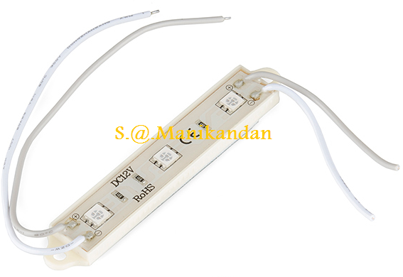
LED Light Bars are a super-easy way to add some extra-bright and colorful illumination to your project. Each Light Bar is essentially a set of three super-bright 5050-size LEDs. They’re offered in a variety of colors including white, red, blue, and green (note: the blue and green light bars are an older version, they
look different but can still be connected the same way).
 While these bars are very simple devices, they do have a few quirks when it comes to using them. Like the fact that their nominal operating voltage is 12V. In this tutorial we’ll go over some of the important specifications of these LED Light Bars.

Hardware Overview

A glance at the LED Bars will reveal that there’s not a whole lot required to interface with them. There are two pairs of wire pigtails coming off the sides, labeled ‘+’ and ‘-’. The darker-gray wire connects to the ‘+’ pin, and the white wire connects to ‘-’ on both sides.

 These wires supply power directly to the LEDs. A nominal voltage of 12V should be applied to these wires. A lower voltage will work (to a point) but result in dimmer LEDs. Either of the wire pairs can be used to supply power to the LED, and the unused pair can either be trimmed or connected to another LED bar.

For mounting purposes there are drill holes on either side of the board, and a peel-away sticky foam on the backside.

LED Characteristics

The “nominal” voltage for these LED Bars is 12V. “Nominal” as in that’s what’s recommended by the manufacturer. They will work at lower voltages, although that’ll mean sacrificing some brightness.
The table below shows some of the characteristics for each of the LED bar colors. These are values we found while testing the bars out. The minimum voltage was the lowest voltage where the LEDs were at recognizably lit up, although very dim. We recommend that you at least give the LEDs around 7V. The higher the voltage, the brighter your LED will be.

As far as current pull goes, both LED colors consume about the same when powered from between 9 and 12V, up to about 55mA when powered at the nominal voltage.

Light Bar Circuit

Looking at the visible components on the bars, it’s apparent that there’s not a lot to them. Three six-pin, SMD LEDs, and an equal number of resistors. We can easily reverse-engineer this circuit to find out exactly how these things work.

Each SMD LED is actually a collection of three equal LEDs. The LED bar’s PCB is set up to string those LEDs in series, with the resistor in-line to limit current. The values of the resistors depend on the color of the Bar. The red bar, for example uses 330Ω,301Ω,151Ω,241Ω and the white bar uses 150Ω resistors.
Connect three of those circuits in parallel an you have your LED bar!

Assembly tips

In most cases, Light Bar assembly begins with stripping some wire. The wire pigtails on the bars are 20 AWG, and should be easy enough to strip with any, old wire stripper.
The wire lengths can be extended, if need be, with a little splice. Don’t forget to cover your splice with heatshrink!
Alternatively the stripped pigtails can be tinned, crimped, or plugged directly into a mating connector.

Stringing bars

The ‘+’ and ‘-’ wires of one bar can be connected to another to string them together. More and more bars can be stringed until you start to approach the current limit of the 20 AWG wires – about 1.5A. With some back of the napkin calculations – 55mA per bar, 1.5A max – that’d be 25-ish bars.

Mounting the bars

There are two possible methods for mounting the LED bars. There are mounting holes on either end of the bar with a 0.15" drill diameter, allowing for the bars to be screwed down. Every bar also includes a peel-away sticky-foam backing which adheres about as well as you could expect.
With a little prying, the PCB assembly part of the LED bar can be removed from the plastic mounting backing. This might be useful if your boards might need a tighter fit.


Example Circuits

 There are a variety of ways these LED bars can be controlled and illuminated. Let’s look at a few example circuits:

Direct Power

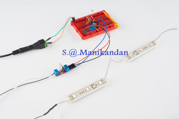
If you don’t care about dimming the LEDs, the easiest way to power them up is to connect them directly to a 12V power supply. Stick them in your enclosure or project, plug the supply in, and forget about them. If you’re looking for a supply that can source 12V,
The DC Terminal Adapter makes connecting the 12V wall wart to the LED bar way easy.
To gain a little control over the LEDs, you can add a switch in-line between the power source and either the ‘+’ or ‘-’ wire of the first LED bar.
 

Dimming with MOSFET Using a 555 Timer

If you want to add some dimming control over your LED bar, MOSFETs combined with pulse width modulation are the tools you’ll need. There are a few approaches you can take to generating a PWM signal to control the MOSFET and LED bar. Here are a couple options: 
control the LED bars via PWM. Use a circuit like below, with an n-channel MOSFET  use a 555 timer and a handful of common components to generate the PWM signal. Here’s an example circuit:
 Most 555 timers can work at up to 16V, so you can run it directly off the 12V supply. Then twist the potentiometer to adjust the brightness.

LED Light bar applications


 Application: 
                   === > Led module + back light for sign

                   === > Back lighting for advertising signs,channel letters,light boxes,etc.
                   === > Widely used indoor/outdoor advertising sign, channel letter & signs with non-waterproof requirements
                   === > Ideal for small channel letter & lighting box


 Specifications:


Led type
5050smd
Led quantity
3pcs
Size
75*12*4mm
Material
Plastic
Input voltage
DC12V
Current
60mA
Power
0.72W
Color
Red/Blue/Green/White/RGB
Viewing angle
120°
Lumen
60-66lm
Working temperature
-20℃--60℃
Storing temperature
-25℃--80℃
Certification
CE/Rohs

 Lighting pictures:
Installation Instruction:

LED Polarity :

smd led strip

 Led data sheet

                            
Forwatd Voltage            =    2.8 ~ 3.5 DC
Forward Current            =     60 mA
Lumens / LED                =    18.5 ~ 22.5 Lumens
Beam Angle (Degrees)    =    120
Power                             =  0.2 w